| CPC H10K 59/65 (2023.02) [G06F 3/04166 (2019.05); G06V 40/1318 (2022.01); G09G 3/3233 (2013.01); H10K 59/121 (2023.02); H10K 59/131 (2023.02); G09G 2300/0842 (2013.01); G09G 2354/00 (2013.01)] | 16 Claims |
|
1. A display panel, comprising:
a base substrate with a display area; wherein:
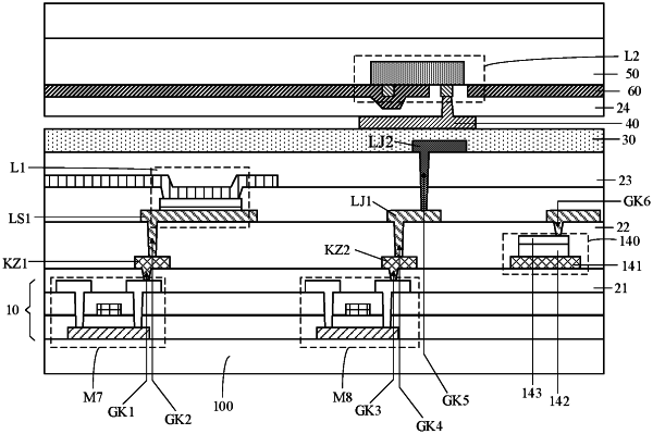
the display area comprises a plurality of sub-pixels; the display area comprises a recognition area; each sub-pixel in the recognition area comprises: a pixel driving circuit, a first control circuit, a second control circuit, an organic light emitting diode, a micro light emitting diode and a photoelectric converter;
in each sub-pixel, the organic light emitting diode is electrically connected with the pixel driving circuit through the first control circuit, and the micro light emitting diode is electrically connected with the pixel driving circuit through the second control circuit; and
the photoelectric converter is configured to receive light which is emitted by the micro light emitting diode and is reflected by a finger;
wherein the display panel further comprises:
a driving array layer, positioned on the base substrate, and the driving array layer comprises the pixel driving circuit, the first control circuit and the second control circuit;
a first insulating layer, positioned on a side, facing away from the base substrate, of the driving array layer;
a photoelectric device layer, positioned on a side, facing away from the base substrate, of the first insulating layer; and the photoelectric device layer comprises the photoelectric converter;
a second insulating layer, positioned on a side, facing away from the base substrate, of the photoelectric device layer;
a first light emitting structure layer, positioned on a side, facing away from the base substrate, of the second insulating layer, and the first light emitting structure layer comprises the organic light emitting diode;
a third insulating layer, positioned on a side, facing away from the base substrate, of the first light emitting structure layer; and
a second light emitting structure layer, positioned on a side, facing away from the base substrate, of the third insulating layer, and the second light emitting structure layer comprises the micro light emitting diode.
|