| CPC H10K 59/40 (2023.02) [G06F 3/0446 (2019.05); H10K 50/844 (2023.02); H10K 50/858 (2023.02); H10K 50/865 (2023.02); H10K 59/123 (2023.02)] | 20 Claims |
|
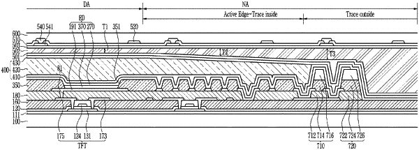
1. A display device comprising:
a display area and a non-display area;
a light emitting element disposed on the display area of a substrate;
a dam disposed on the non-display area of the substrate;
an encapsulation layer disposed on the light emitting element and the dam;
a planarization layer disposed on the encapsulation layer;
a sensing electrode disposed on the planarization layer; and
an opening area disposed in the display area; and
an opening periphery area surrounding the opening area, wherein
a thickness of a portion of the planarization layer disposed in the opening periphery area is greater than a thickness of a portion of the planarization layer disposed in the display area.
|