| CPC H10K 59/40 (2023.02) [H10K 50/8426 (2023.02); H10K 59/131 (2023.02); H10K 71/00 (2023.02); H10K 59/1201 (2023.02)] | 16 Claims |
|
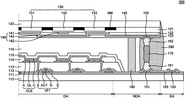
1. An organic light emitting display device comprising:
a lower substrate including a plurality of sub-pixels, the lower substrate having a display area, a non-display area enclosing the display area, and an exposed area extending from one side of the non-display area;
a lower touch pad unit formed in the non-display area, the lower touch pad unit adjacent to the exposed area on the lower substrate;
an upper substrate opposite to a remaining area excluding the exposed area of the lower substrate;
an upper touch pad unit on the upper substrate, the upper touch pad unit corresponding to the lower touch pad unit;
a first connection electrode in direct contact with the lower touch pad unit;
a second connection electrode opposite to the first connection electrode and in direct contact with the upper touch pad unit;
a self-assembly contact member disposed between the first connection electrode and the second connection electrode, the self-assembly contact member electrically connecting together the first connection electrode and the second connection electrode; and
a first connection pad unit and a second connection pad unit in the exposed area of the lower substrate,
wherein the first connection pad unit is connected to a thin film transistor formed in the display area of the lower substrate, and the second connection pad unit is connected to the lower touch pad unit.
|