| CPC H10K 59/40 (2023.02) [G06F 3/044 (2013.01); G06F 3/0412 (2013.01); G06F 3/0443 (2019.05); G06F 3/0446 (2019.05); G06F 3/04164 (2019.05); H10K 50/844 (2023.02); H10K 50/865 (2023.02); H10K 59/131 (2023.02); H10K 59/38 (2023.02); H10K 77/111 (2023.02); H10K 2102/311 (2023.02)] | 24 Claims |
|
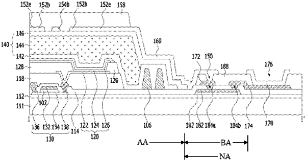
1. An organic light-emitting display device comprising:
a substrate;
a thin-film transistor including a semiconductor layer on the substrate, a gate electrode overlapping the semiconductor layer with a gate insulating film interposed therebetween, and source and drain electrodes contacting the semiconductor layer through a contact hole of a n interlayer layer;
a light-emitting element disposed on the thin-film transistor;
an encapsulation unit disposed on the light-emitting element;
a touch sensor disposed on the encapsulation unit; and
a touch protective film disposed on the touch sensor,
wherein the touch sensor comprises:
first touch electrodes arranged on the encapsulation unit in a first direction, the first touch electrodes being connected to each other via first bridges;
second touch electrodes arranged on the encapsulation unit in a second direction, the second touch electrodes being connected to each other via second bridges;
a routing line connected to each of the first touch electrodes and the second touch electrodes, the routing line being disposed on a lateral surface of the encapsulation unit; and
a touch pad connected to the routing line via a first upper connection electrode, a second upper connection electrode and a lower connection electrode,
wherein the first and second bridges and the first and second touch electrodes are formed of a same material as each other in a same plane, and the first and second bridges and the first and second touch electrodes are coplanar and disposed directly on an uppermost layer of the encapsulation unit,
wherein none of the first bridges bisect and overlap any of the second bridges,
wherein the touch protective film is a single layer and is in contact with upper surfaces of both of the first and second bridges,
wherein the lower connection electrode is formed of a same material a s the gate electrode,
wherein the first upper connection electrode and the second upper connection electrode are disposed on the interlayer layer covering the gate electrode, the semiconductor layer and the lower connection electrode, and a portion of the interlayer layer separates the first upper connection electrode and the second upper connection electrode at a non-active area of the substrate,
wherein the first upper connection electrode electrically connects the lower connection electrode and the routing line via a routing contact hole formed in a crack prevention layer and a connection contact hole formed in the interlayer layer, and the second upper connection electrode electrically connects the lower connection electrode and the touch pad,
wherein the routing contact hole and the connection contact hole are vertically aligned in the non-active area of the substrate, and
wherein the crack prevention layer is located in a bending area located at a portion of the non-active area, and
wherein the routing contact hole is located only in the bending area.
|