| CPC H10K 59/353 (2023.02) [G09G 3/3233 (2013.01); H10K 59/126 (2023.02); H10K 59/131 (2023.02); H10K 59/352 (2023.02); G09G 2300/0452 (2013.01); G09G 2300/0842 (2013.01); H10K 59/1201 (2023.02)] | 20 Claims |
|
1. A display panel, comprising: a substrate, a first shielding layer, a plurality of sub-pixel areas arranged in an array, and a plurality of sub-pixel driving circuits corresponding to the plurality of sub-pixel areas in a one-to-one manner, wherein
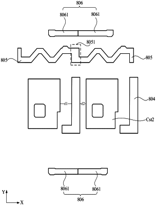
each of the plurality of sub-pixel driving circuits includes a driving transistor and a storage capacitor, the storage capacitor includes a first electrode plate and a second electrode plate arranged opposite to each other, and the first electrode plate is located between the substrate and the second electrode plate,
the first shielding layer includes a first shielding pattern located in each of the plurality of sub-pixel areas, the first shielding pattern and the second electrode plate are arranged at a same layer, and the first shielding pattern is located between two adjacent second electrode plates of two adjacent sub-pixel areas,
the first shielding pattern and the second electrode plate are alternately arranged along a first direction, a projection of the first shielding pattern on a line extending along the first direction does not overlap a projection of the second electrode plate on the line extending along the first direction, and a projection of the first shielding pattern on a line extending along a second direction overlaps a projection of the second electrode plate on the line extending along the second direction, and the first direction intersects the second direction.
|