| CPC H10K 59/131 (2023.02) [G09G 3/3258 (2013.01); H10K 59/1201 (2023.02)] | 15 Claims |
|
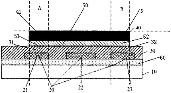
1. An array substrate, comprising:
a base substrate; and
a wiring layer and a light-emitting layer which are stacked on the base substrate sequentially, wherein the wiring layer comprises a signal wiring, a first wiring, and a second wiring,
wherein a projection of the first wiring on the base substrate is separated from a projection of the second wiring on the base substrate, and the first wiring and the second wiring are respectively disposed on two sides of the light-emitting layer below the light-emitting layer;
wherein the signal wiring is located between the first wiring and the second wiring, and the projection of the first wiring on the base substrate and the projection of the second wiring on the base substrate are respectively overlapped with projections of two edges of the light-emitting layer on the base substrate;
wherein a length of the second wiring is less than a length of the signal wiring in an extension direction of the signal wiring; and
wherein a length of a portion of the projection of the first wiring on the base substrate overlapping with a projection of the light-emitting layer on the base substrate in the extension direction of the signal wiring is substantially equal to a length of a portion of the projection of the second wiring on the base substrate overlapping with the projection of the light-emitting layer on the base substrate in the extension direction of the signal wiring.
|