| CPC H10K 59/131 (2023.02) [G06F 3/0412 (2013.01); G09G 3/3225 (2013.01); G09G 3/3266 (2013.01); G06F 3/044 (2013.01); G06F 2203/04112 (2013.01); G09G 2300/0439 (2013.01); G09G 2300/0819 (2013.01); G09G 2300/0842 (2013.01); G09G 2300/0861 (2013.01)] | 18 Claims |
|
1. A display device, comprising:
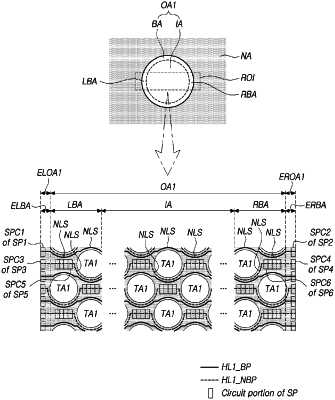
a display panel including a plurality of subpixels and a plurality of signal lines, the display panel defining a display area having a first optical area and a normal area located outside of the first optical area, and a non-display area, wherein the first optical area comprises a plurality of light emitting areas and a plurality of first transmission areas, and wherein the normal area comprises a plurality of light emitting areas,
wherein the display panel includes a plurality of first horizontal lines among the plurality of signal lines disposed through the first optical area, and
wherein the first horizontal lines include a bypass line connected to subpixels at both boundaries of the first optical area and not connected to other subpixels inside of the first optical area, and a non-bypass line connected to the subpixels at both boundaries of the first optical area and the subpixels inside of the first optical area,
wherein each of the plurality of subpixels includes:
a light emitting element having an anode electrode, an emission layer, and a cathode electrode;
a driving transistor configured to drive the light emitting element, the driving transistor having a first node, a second node, and a third node;
a first transistor configured to control a connection between the first node and the second node, the first transistor configured to be controlled by a first scan signal;
a second transistor configured to control a connection between the third node and a data line, the second transistor configured to be controlled by a second scan signal;
a third transistor configured to control a connection between the third node and a driving voltage line, the third transistor configured to be control by an emission control signal;
a fourth transistor configured to control a connection between the anode electrode and the second node, the fourth transistor configured to control by the emission control signal;
a fifth transistor configured to control a connection between an initialization signal line and the second node, the fifth transistor configured to be controlled by a third scan signal;
a sixth transistor configured to control a connection between an anode reset voltage line and the anode electrode; and
a storage capacitor connected between the first node and the driving voltage line, and
wherein the plurality of first horizontal lines includes a first scan line configured to supply the first scan signal, a second scan line configured to supply the second scan signal, a third scan line configured to supply the third scan signal, and an emission control line configured to supply the emission control signal.
|