| CPC H10K 59/131 (2023.02) [H10K 59/1213 (2023.02); H10K 59/1216 (2023.02); H10K 59/1315 (2023.02)] | 20 Claims |

|
1. A display substrate, comprising: a base substrate, and a first wiring layer, a second wiring layer, a third wiring layer, a fourth wiring layer and a pixel electrode layer successively away from the base substrate, an insulating layer is disposed between any adjacent ones of the first wiring layer, the second wiring layer, the third wiring layer, the fourth wiring layer and the pixel electrode layer, a reset control line and a light emitting control line, which each extend in a row direction, are disposed in the first wiring layer,
the display substrate further comprises a first reference voltage line, a second reference voltage line, and a first reference voltage auxiliary line, the first reference voltage line and the first reference voltage auxiliary line are respectively disposed in one of the second wiring layer, the third wiring layer, and the fourth wiring layer, the first reference voltage line and the first reference voltage auxiliary line extend in different directions, the second reference voltage line and the first reference voltage auxiliary line extend in a same direction, the first reference voltage auxiliary line is electrically coupled to the first reference voltage line through a plurality of via holes penetrating through the insulating layer between a layer where the first reference voltage auxiliary line is disposed and a layer where the first reference voltage line is disposed, via a coupling line extending in the same direction as the first reference voltage line,
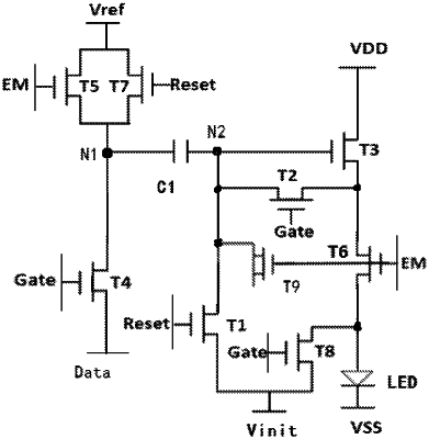
the display substrate further comprises a first capacitor, the first reference voltage auxiliary line and the first reference voltage line are configured to provide a reset voltage to a first electrode of the first capacitor, and the second reference voltage line is configured to provide a reset voltage to a pixel electrode in the pixel electrode layer.
|