| CPC H10K 59/131 (2023.02) [H01L 25/18 (2013.01); H10K 59/1213 (2023.02); H10K 59/1216 (2023.02); H10K 59/352 (2023.02); H01L 27/1255 (2013.01)] | 20 Claims |
|
1. A display substrate, comprising:
a base having a display area;
a plurality of data lines disposed on the base and located in the display area; and
a plurality of columns of pixel driving circuits disposed on the base and located in the display area; a column of pixel driving circuits in the plurality of columns of pixel driving circuits being connected to a corresponding data line in the plurality of data lines, each pixel driving circuit in the column of pixel driving circuits including a driving transistor and a first transistor electrically connected to the driving transistor, the driving transistor being a P-type transistor, and the first transistor including:
a first active pattern having a first channel region, and a first doped region and a second doped region that are located on two opposite sides of the first channel region;
a first gate, an orthographic projection of the first gate on the base overlapping with an orthographic projection of the first channel region on the base; and
a first insulating block disposed on a side of the first active pattern away from the base, the first insulating block being a portion of an insulating layer located in a region where the first transistor is located, and the first insulating block having a first via; the data line being electrically connected to a portion of the first active pattern located in the first doped region through the first via;
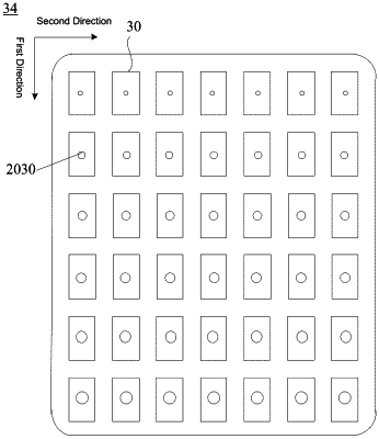
wherein sizes of all first vias in the column of pixel driving circuits gradually decrease in a first direction, and the first direction is a direction where a signal input terminal of the data line points to a distal end opposite to the signal input terminal.
|