| CPC H10K 59/122 (2023.02) [H10K 71/00 (2023.02); H10K 59/1201 (2023.02)] | 20 Claims |
|
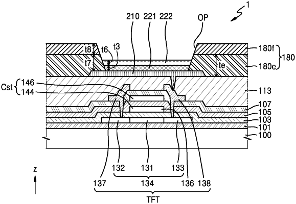
1. A method of manufacturing a display device, the method comprising:
forming a first electrode on a substrate;
forming a bank layer on the first electrode, wherein the bank layer includes an opening portion exposing at least a portion of the first electrode;
forming a first bank layer and a second bank layer by baking the bank layer, wherein the second bank layer is on the first bank layer and has liquid repellency;
forming a first layer on the first electrode; and
forming a third bank layer and a fourth bank layer by baking the first bank layer and the second bank layer, wherein the fourth bank layer is on the third bank layer and has liquid repellency,
wherein the fourth bank layer is thinner than the second bank layer.
|