| CPC H10K 59/122 (2023.02) [H10K 71/00 (2023.02)] | 12 Claims |
|
1. A display panel, comprising a substrate, as well as a pixel defining layer and a cathode layer that are laminated on the substrate,
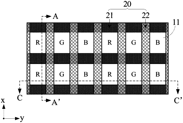
wherein the pixel defining layer comprises a plurality of strip-shaped first pixel defining structures and a plurality of strip-shaped second pixel defining structures, the plurality of first pixel defining structures and the plurality of second pixel defining structures are arranged in a crossed fashion to define a plurality of sub-pixel regions arranged in an array on the substrate, any adjacent first pixel defining structures and any adjacent second pixel defining structures enclosing one sub-pixel region; and
wherein a slope angle of the second pixel defining structure is greater than a slope angle of the first pixel defining structure, and the second pixel defining structure is configured to separate portions of the cathode layer on two sides of the second pixel defining structure; a portion of the cathode layer between adjacent second pixel defining structures is of a continuous strip-shaped structure;
the display panel further comprises sub-pixels of at least two colors,
wherein the sub-pixels in sub-pixel regions between adjacent second pixel defining structures are of the same color, and the sub-pixels in any adjacent sub-pixel regions between adjacent first pixel defining structures are of different colors;
the display panel further comprises:
a plurality of anode blocks disposed between the pixel defining layer and the substrate, wherein the plurality of anode blocks are in one-to-one correspondence with the plurality of sub-pixel regions, for each of the anode blocks, a central part of the anode block is disposed in a sub-pixel region corresponding to the anode block, and in a direction perpendicular to the substrate, the pixel defining layer directly contacts and covers an edge part of the anode block; and
a pixel driving circuit disposed within the substrate and electrically connected to each of the anode blocks, wherein the pixel driving circuit comprises at least one oxide transistor, and the first pixel defining structure is lightproof and covers the pixel driving circuit, to avoid light rays from irradiating to the at least one oxide transistor in the pixel driving circuit;
the slope angle of the first pixel defining structure ranges from 20 degrees to 60 degrees, and the slope angle of the second pixel defining structure ranges from 90 degrees to 100 degrees.
|