| CPC H10K 59/122 (2023.02) [H10K 59/38 (2023.02); H10K 71/00 (2023.02); H10K 59/1201 (2023.02)] | 16 Claims |
|
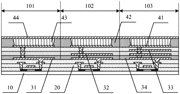
1. A display substrate, comprising a plurality of pixel units arranged in a matrix, wherein the pixel units each comprise a plurality of sub-pixels, the sub-pixels each comprise a silicon substrate and a micro-cavity modulation layer and an emitting structure layer, the micro-cavity modulation layer is provided with a reflective electrode, the emitting structure layer comprises a first electrode, an emitting layer and a semi-transparent and semi-reflective second electrode which are sequentially disposed on the micro-cavity modulation layer, and distance between the second electrode and the reflective electrode is different in each sub-pixel; wherein
the pixel units each comprise a first sub-pixel, a second sub-pixel and a third sub-pixel adjacently arranged;
the first sub-pixel, the second sub-pixel and the third sub-pixel respectively comprise a first reflective electrode, a second reflective electrode and a third reflective electrode;
each of the second reflective electrode and the third reflective electrode is electrically connected to a drive transistor through a first connection electrode provided in a same layer as the first reflective electrode;
in the first sub-pixel, an orthographic projection of the drive transistor on the silicon substrate is located within an orthographic projection of the first reflective electrode on the silicon substrate;
in each of the second sub-pixel and the third sub-pixel, an orthographic projection of the drive transistor on the silicon substrate is located within an orthographic projection of the first connecting electrode on the silicon substrate;
wherein the sub-pixels each further comprise a driving circuit layer disposed on the silicon substrate, the micro-cavity modulation layer is disposed on the driving circuit layer, the driving circuit layer comprises the driving transistor having a drain electrode;
the micro-cavity modulation layer of the first sub-pixel comprises:
the first reflective electrode disposed on the driving circuit layer, wherein the first reflective electrode is connected with the drain electrode of the driving circuit layer through a first via provided in the driving circuit layer;
a first modulation layer covering the first reflective electrode, wherein the first modulation layer is provided with a second via exposing the first reflective electrode;
a first connection block disposed in the second via, wherein the first connection block is connected with the first reflective electrode;
a second modulation layer covering the first modulation layer and the first connection block, wherein the second modulation layer is provided with a third via exposing the first connection block;
a second connection block disposed in the third via, wherein the second connection block is connected with the first connection block; and
a third modulation layer covering the second modulation layer and the second connection block, wherein the third modulation layer is provided with a fourth via exposing the second connection block.
|