| CPC H10K 59/1213 (2023.02) [G09G 3/3233 (2013.01); H10K 50/805 (2023.02); H10K 50/81 (2023.02); H10K 59/121 (2023.02); H10K 59/1216 (2023.02); H10K 59/131 (2023.02); G09G 2300/0426 (2013.01); G09G 2310/02 (2013.01); G09G 2340/0407 (2013.01); H01L 27/124 (2013.01); H01L 27/1214 (2013.01)] | 25 Claims |
|
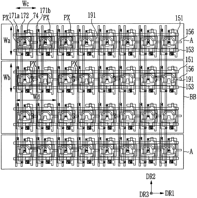
1. A display device, comprising:
a first display area including a plurality of first pixel electrodes; and
a second display area including a plurality of second pixel electrodes, wherein:
a first pitch in a first direction of the plurality of first pixel electrodes in the first display area is smaller than a second pitch in the first direction of the plurality of second pixel electrodes in the second display area,
a length in the first direction of the first pixel electrodes in the first display area is smaller than a length in the first direction of the second pixel electrodes in the second display area, and
the timber of transistors disposed in the first display area is different from the number of transistors disposed in the second display area.
|