| CPC H10K 59/1213 (2023.02) [H10K 59/123 (2023.02); H10K 59/126 (2023.02); H10K 59/1216 (2023.02); H10K 77/111 (2023.02); H01L 27/1225 (2013.01); H01L 27/1251 (2013.01); H01L 27/1255 (2013.01); H01L 27/1259 (2013.01); H01L 29/24 (2013.01); H01L 29/66757 (2013.01); H01L 29/66969 (2013.01); H01L 29/7869 (2013.01); H01L 29/78633 (2013.01); H01L 29/78648 (2013.01); H01L 29/78675 (2013.01); H10K 59/1201 (2023.02); H10K 2102/311 (2023.02)] | 3 Claims |
|
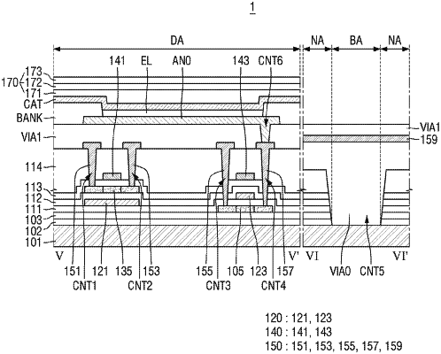
1. A display device comprising:
a base substrate having a display region and a non-display region adjacent to the display region, the display region including a first region and a second region;
a first semiconductor layer at the second region of the base substrate, the first semiconductor layer comprising polysilicon;
a first insulating layer on the first semiconductor layer;
a first conductive layer on the first insulating layer, the first conductive layer comprising a bottom gate electrode at the first region and a second-first gate electrode at the second region;
a second insulating layer on the first conductive layer;
a second semiconductor layer on the second insulating layer at the first region, the second semiconductor layer comprising an oxide;
a third insulating layer on the second semiconductor layer;
a second conductive layer on the third insulating layer, the second conductive layer comprising a top gate electrode at the first region;
a fourth insulating layer on the second conductive layer;
a third conductive layer on the fourth insulating layer, the third conductive layer comprising a first source electrode, a first drain electrode, a second source electrode, and a second drain electrode, each of the first source electrode and the first drain electrode being connected to the second semiconductor layer, and each of the second source electrode and the second drain electrode being connected to the first semiconductor layer; and
a cap conductive pattern at the second region between the second insulating layer and the third insulating layer,
wherein the cap conductive pattern, the second-first gate electrode, and the second insulating layer that is between the cap conductive pattern and the second-first gate electrode define a capacitor, and
wherein the third insulating layer covers the cap conductive pattern at the second region, and is located between the top gate electrode of the second conductive layer and the second semiconductor layer at the first region.
|