| CPC H10K 59/1213 (2023.02) [H10K 59/1216 (2023.02); H10K 59/131 (2023.02); H10K 71/00 (2023.02); H01L 27/1255 (2013.01); H10K 59/1201 (2023.02)] | 19 Claims |
|
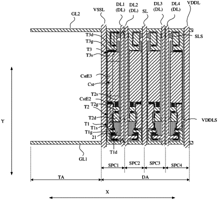
1. A display panel, comprising:
a base substrate; and
a pixel arranged on the base substrate, comprising a light-transmitting area and a display area arranged side by side in a first direction parallel to the base substrate, wherein the pixel comprises a plurality of sub-pixel drive circuits sequentially arranged in the first direction in the display area, each of the sub-pixel drive circuits comprises a switching transistor, a detection transistor and a storage capacitor, the switching transistor and the detection transistor are respectively located on both sides of the storage capacitor in a second direction perpendicular to the first direction and parallel to the base substrate;
a first gate line configured to provide a first scanning signal to the plurality of sub-pixel drive circuits; and
a second gate line configured to provide a second scanning signal to the plurality of sub-pixel drive circuits,
wherein the first gate line and the second gate line are respectively located on both sides of the light-transmitting area, the first gate line is located on a side of the switching transistor away from the storage capacitor, the second gate line is located on a side of the detection transistor away from the storage capacitor, and between two ends of the pixel in the first direction, at least one of the first gate line and the second gate line is linear and extends in the first direction.
|