US 11,903,250 B2
Display apparatus and method of manufacturing the same
Seungjin Lee, Yongin-si (KR); Sanghoon Kim, Yongin-si (KR); Jongsung Park, Yongin-si (KR); and Sangshin Lee, Yongin-si (KR)
Assigned to Samsung Display Co., Ltd., Yongin-si (KR)
Filed by Samsung Display Co., Ltd., Yongin-si (KR)
Filed on Jul. 28, 2021, as Appl. No. 17/443,937.
Claims priority of application No. 10-2020-0129600 (KR), filed on Oct. 7, 2020.
Prior Publication US 2022/0109122 A1, Apr. 7, 2022
Int. Cl. H01L 51/52 (2006.01); H01L 51/56 (2006.01); H01L 27/32 (2006.01); H10K 59/121 (2023.01); H10K 50/81 (2023.01); H10K 59/35 (2023.01); H10K 71/00 (2023.01); H10K 71/16 (2023.01); C23C 14/04 (2006.01); H10K 50/11 (2023.01); H10K 59/122 (2023.01); H10K 59/12 (2023.01); H10K 102/00 (2023.01)
CPC H10K 59/121 (2023.02) [C23C 14/042 (2013.01); H10K 50/81 (2023.02); H10K 59/353 (2023.02); H10K 71/00 (2023.02); H10K 71/166 (2023.02); H10K 50/11 (2023.02); H10K 59/1201 (2023.02); H10K 59/122 (2023.02); H10K 59/352 (2023.02); H10K 2102/341 (2023.02)] 19 Claims
OG exemplary drawing
 
1. A display apparatus comprising:
a substrate;
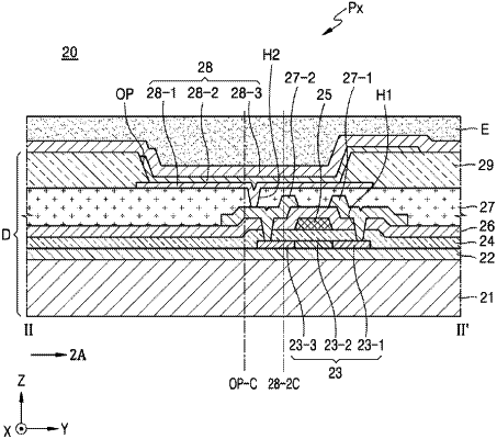
a pixel definition layer over the substrate, the pixel definition layer comprising at least one opening area; an
an organic emission layer over the pixel definition layer and covering the opening area,
wherein a center of the opening area and a center of the organic emission layer are at different positions in plan view, and
wherein an end of the organic emission layer overlaps the opening area in plan view.