| CPC H10K 59/121 (2023.02) [H10K 50/844 (2023.02); H10K 59/131 (2023.02); H10K 59/38 (2023.02); H10K 71/00 (2023.02); H10K 59/1201 (2023.02)] | 20 Claims |
|
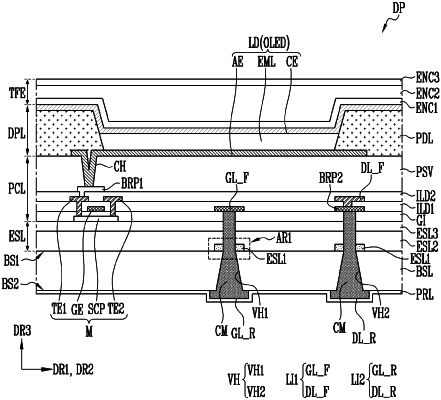
1. A display device comprising:
a base layer, the base layer including a first surface and a second surface;
pixels and first lines that are disposed on the first surface;
second lines disposed on the second surface and corresponding to the first lines;
a multi-layered etch stopper layer disposed on the first surface and disposed between the base layer and the first lines; and
via holes penetrating the base layer and the multi-layered etch stopper layer, the via holes connecting the first lines to the second lines,
wherein the multi-layered etch stopper layer includes:
a first etch stopper layer disposed on the first surface and surrounding each of the via holes, the first etch stopper layer including an inorganic layer; and
a second etch stopper layer disposed on the first surface and completely covering the first etch stopper layer, the second etch stopper layer being open in a region corresponding to the via holes, and wherein
each of the via holes has an opening at the second surface of the base layer that is larger than an opening at the first surface of the base layer.
|