| CPC H10K 59/12 (2023.02) [H01L 21/02057 (2013.01); H01L 21/02532 (2013.01); H01L 21/02592 (2013.01); H01L 21/02675 (2013.01); H01L 29/66757 (2013.01); H01L 29/78675 (2013.01)] | 8 Claims |
|
1. A display device, comprising:
a substrate;
a thin film transistor disposed on the substrate; and
a display element disposed on the thin film transistor,
wherein:
the thin film transistor comprises:
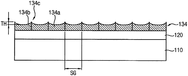
an active pattern disposed on the substrate and including a plurality of grains separated by grain boundaries, and having protrusions formed at the grain boundaries, the active pattern having a low surface roughness with a root-mean-square (RMS) value of about 4 nm or less, wherein the thin film transistor has a substantially uniform threshold voltage;
a gate insulation layer disposed on the active pattern, the gate insulation layer having a thickness in a range of about 30 nm to about 200 nm, and being protected from damage by the low surface roughness of the active pattern; and
a gate electrode disposed on the gate insulation layer.
|