| CPC H10K 59/00 (2023.02) [G01K 7/183 (2013.01); G01L 1/2293 (2013.01); H10K 59/131 (2023.02); H10K 59/88 (2023.02); H10K 50/844 (2023.02); H10K 59/122 (2023.02)] | 25 Claims |
|
1. An electronic device, comprising:
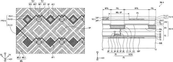
a base substrate including an active region, which includes a sensing region, and a peripheral region adjacent to the active region;
an input sensor comprising a plurality of first sensing electrodes, a plurality of second sensing electrodes, which are on the base substrate, the second sensing electrodes being spaced apart from the first sensing electrodes, and a plurality of dummy patterns spaced apart from the first sensing electrodes and the second sensing electrodes; and
a pressure sensor comprising a plurality of strain sensing patterns overlapping the sensing region, and a plurality of strain connection patterns connecting the strain sensing patterns to each other,
wherein the strain sensing patterns and the dummy patterns are at a same layer, and
wherein the strain sensing patterns are spaced apart from the first sensing electrodes and the second sensing electrodes when viewed in a plan view.
|