| CPC H10K 50/865 (2023.02) [H10K 59/38 (2023.02); H10K 71/00 (2023.02)] | 13 Claims |
|
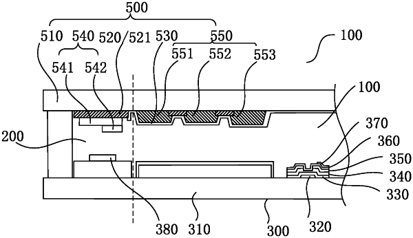
1. A display panel, comprising a display area and a non-display area, the display panel comprising:
a first substrate; and
a second substrate, disposed opposite to the first substrate;
wherein the first substrate comprises a mark corresponding to the non-display area;
the second substrate comprises a light shielding portion corresponding to the non-display area, and the light shielding portion comprises a blocking member corresponding to the mark.
wherein the second substrate sequentially comprises a second base, a light shielding layer, a color filter layer, the blocking member, and a common electrode layer, wherein the light shielding portion and the light shielding layer are formed in a same manufacture process by using a same material;
wherein the blocking member and the color filter layer are formed in the same manufacture process by using a same material.
|