| CPC H10K 50/844 (2023.02) [H10K 59/12 (2023.02); H10K 77/111 (2023.02); H10K 2102/311 (2023.02)] | 6 Claims |
|
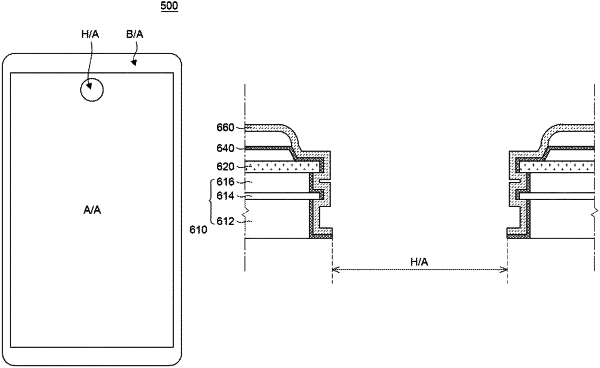
1. A display device, comprising:
a flexible substrate including an active area, and a non-active area adjacent to the active area;
a thin-film transistor on the active area;
a light-emitting element coupled to the thin-film transistor on the active area;
an encapsulation layer on the thin-film transistor and the light-emitting element;
a hole in the active area, the hole having a side surface abutting the encapsulation layer;
a first common layer including at least one or more components of the thin-film transistor; and
a second common layer including at least one or more components of the light-emitting element,
wherein the flexible substrate includes a first substrate laver, a second substrate layer disposed on the first substrate layer, and a substrate protecting layer between the first substrate layer and the second substrate layer,
wherein the second common layer is on the first common layer, wherein the first common layer includes a first tip, the first tip having a top surface, a bottom surface opposite the top surface, and a side surface between the top surface and the bottom surface, the first tip protruding further horizontally than a side surface of the second substrate layer adjacent to the first tip, the first tip and the side surface of the second substrate layer forming a first undercut region,
wherein the substrate protecting layer includes a second tip, the second tip having a top surface, a bottom surface opposite the top surface, and a side surface between the top surface and the bottom surface, the second tip protruding further horizontally than a side surface of the first substrate layer adjacent to the second tip, the second tip and the side surface of the first substrate layer forming a second undercut region,
wherein the second common layer extends continuously from the top surface of the first tip to the side surface of the first tip, covers an entirety of the side surface of the first tip from a lateral direction, and is laterally adjacent to the side surface of the second substrate,
the second common layer extends continuously from the side surface of the second substrate layer to the side surface of the second tip and covers an entirety of the side surface of the second tip from the lateral direction, and
the second common layer covers the side surface of the first substrate layer from the lateral direction,
wherein at least a portion of the bottom surface of the first tip is not covered by the second common layer in the first undercut region and at least a portion of the bottom surface of the second tip is not covered by the second common layer in the second undercut region, and
wherein the encapsulation layer is disposed on the second common layer in the non-active area, and is continuously disposed from an upper portion of the second common layer to the side surface of the second substrate layer without being disconnected.
|