| CPC H10K 50/8428 (2023.02) [H10K 50/865 (2023.02); H10K 59/38 (2023.02); H10K 71/00 (2023.02); G09G 3/3233 (2013.01); G09G 3/3275 (2013.01); H10K 50/844 (2023.02); H10K 59/122 (2023.02)] | 10 Claims |
|
1. A display apparatus, comprising:
a first pixel, a second pixel, and a third pixel each configured to emit different colors;
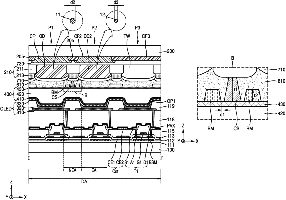
an organic light-emitting diode on a substrate and including a pixel electrode, an intermediate layer, and an opposite electrode;
a black matrix on the organic light-emitting diode;
a column spacer on the same layer as the black matrix and spaced apart from the black matrix by a first distance in a plan view;
a first quantum conversion layer on the substrate to correspond to an emission area of the first pixel and including first quantum dots, and
a partition wall on the black matrix and the column spacer,
wherein the partition wall overlaps the black matrix and the column spacer.
|