| CPC H10B 63/84 (2023.02) [H10B 63/34 (2023.02); H10N 70/011 (2023.02); H10N 70/231 (2023.02); H10N 70/841 (2023.02); H10N 70/8828 (2023.02); H10N 70/8833 (2023.02)] | 5 Claims |

|
1. A method of manufacturing a memory device, the method comprising:
forming a stack structure by repeatedly and alternately depositing a sacrificial layer and an isolating layer on a substrate;
forming a channel hole penetrating through the stack structure;
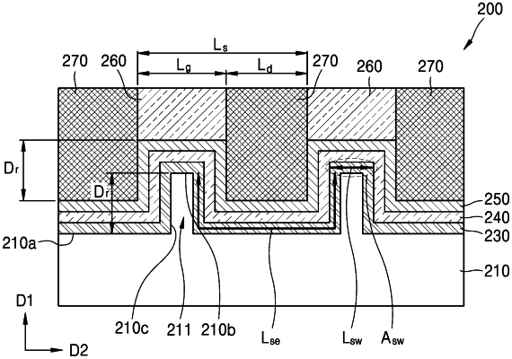
removing a portion of the sacrificial layer such that an inner surface of the channel hole has a concavo-convex shape in a first direction perpendicular to a stack direction of the stack structure;
sequentially forming a gate insulating layer, a channel layer, and a recording material layer on the inner surface of the channel hole;
depositing an insulating material in the channel hole;
forming a gate hole by removing all of a remaining portion of the sacrificial layer; and
depositing an electrode material in the gate hole.
|