| CPC H10B 63/84 (2023.02) [H01L 29/42392 (2013.01); H01L 29/66666 (2013.01); H01L 29/78642 (2013.01); H10B 61/22 (2023.02); H10B 63/34 (2023.02)] | 20 Claims |
|
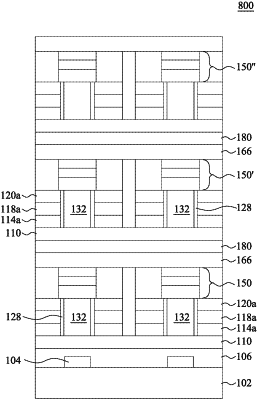
1. A semiconductor device comprising:
a first transistor disposed over a substrate;
a conductive line disposed over the first transistor;
a memory cell disposed over the conductive line, the memory cell including:
a second transistor, wherein the second transistor comprises:
a channel layer;
a gate dielectric layer surrounding a sidewall of the channel layer; and
a gate electrode surrounding a sidewall of the gate dielectric layer; and
a memory element disposed over the second transistor, wherein the second transistor is vertically interjacent the conductive line and the memory element, and wherein the memory element is vertically interjacent the second transistor and a bit line of the memory cell.
|