| CPC H10B 53/30 (2023.02) [H10B 61/10 (2023.02); H10B 63/24 (2023.02); H10B 63/80 (2023.02); H10N 50/01 (2023.02); H10N 70/011 (2023.02)] | 14 Claims |

|
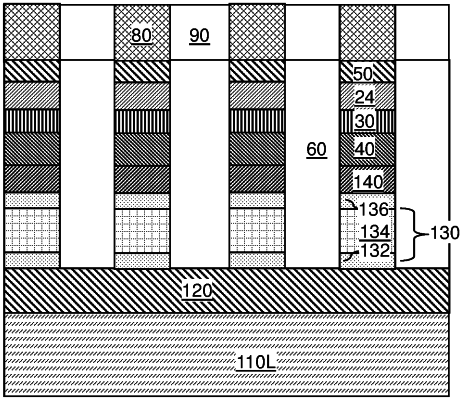
1. A memory device, comprising:
a first electrically conductive line laterally extending along a first horizontal direction;
a memory pillar structure overlying and contacting the first electrically conductive line, wherein the memory pillar structure comprises, from bottom to top:
a stack of a first metallic material plate consisting essentially of a first elemental metal and a second metallic material plate consisting essentially of a second elemental metal and bonded to the first metallic material plate at a bonding interface;
a single crystalline ferroelectric material plate comprising a ferroelectric dielectric metal oxide material having a first single crystalline crystal structure, and
a single crystalline semiconductor plate comprising a semiconductor material having a second single crystalline crystal structure, wherein the second single crystalline crystal structure of the semiconductor material is in epitaxial alignment with the first single crystalline crystal structure of the ferroelectric dielectric metal oxide material at an interface between the semiconductor material and the ferroelectric dielectric metal oxide material; and
a second electrically conductive line laterally extending along a second horizontal direction and overlying and contacting the memory pillar structure.
|