US 11,903,216 B2
Three-dimensional memory device and method
Feng-Cheng Yang, Zhudong Township (TW); Meng-Han Lin, Hsinchu (TW); Sheng-Chen Wang, Hsinchu (TW); Han-Jong Chia, Hsinchu (TW); and Chung-Te Lin, Tainan (TW)
Assigned to TAIWAN SEMICONDUCTOR MANUFACTURING CO., LTD., Hsinchu (TW)
Filed by Taiwan Semiconductor Manufacturing Co., Ltd., Hsinchu (TW)
Filed on May 13, 2022, as Appl. No. 17/744,212.
Application 17/744,212 is a continuation of application No. 17/018,232, filed on Sep. 11, 2020, granted, now 11,355,516.
Claims priority of provisional application 63/052,508, filed on Jul. 16, 2020.
Prior Publication US 2022/0278130 A1, Sep. 1, 2022
Int. Cl. H10B 51/20 (2023.01); H01L 21/3213 (2006.01); H01L 21/768 (2006.01); H01L 23/522 (2006.01); H10B 51/30 (2023.01)
CPC H10B 51/20 (2023.02) [H01L 21/32133 (2013.01); H01L 21/7684 (2013.01); H01L 21/76802 (2013.01); H01L 21/76871 (2013.01); H01L 21/76877 (2013.01); H01L 23/5226 (2013.01); H10B 51/30 (2023.02)] 20 Claims
OG exemplary drawing
 
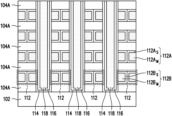
15. A semiconductor device comprising:
a stack of word lines, wherein each word line comprises:
multiple seed layers in physical contact with each other;
multiple conductive elements on opposing sides of the multiple seed layers;
ferroelectric materials adjacent to respective ones of each of the word lines within the stack of word lines; and
semiconductor strips adjacent to respective ones of the ferroelectric materials.