| CPC H10B 51/20 (2023.02) [G11C 11/2255 (2013.01); G11C 11/2257 (2013.01); H10B 51/10 (2023.02); H10B 51/30 (2023.02)] | 20 Claims |

|
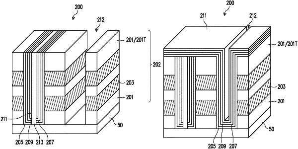
1. A method of forming a ferroelectric random access memory (FeRAM) device, the method comprising:
forming a layer stack over a substrate, wherein the layer stack comprises alternating layers of a first dielectric material and a word line (WL) material;
forming first trenches extending vertically through the layer stack from an upper surface of the layer stack distal from the substrate to a lower surface of the layer stack facing the substrate;
lining bottoms and sidewalls of the first trenches with a ferroelectric material;
forming a channel material in the first trenches over the ferroelectric material;
filling the first trenches with a second dielectric material;
after filling the first trenches, forming second trenches extending vertically through the layer stack, wherein the second trenches are interleaved with the first trenches;
lining bottoms and sidewalls of the second trenches with the ferroelectric material;
forming the channel material in the second trenches over the ferroelectric material;
filling the second trenches with the second dielectric material; and
after filling the second trenches, forming source lines (SLs) and bit lines (BLs) in the first trenches and the second trenches, wherein the SLs and BLs extend vertically through the layer stack.
|