| CPC H10B 51/20 (2023.02) [H10B 43/10 (2023.02); H10B 43/27 (2023.02); H10B 51/10 (2023.02)] | 12 Claims |
|
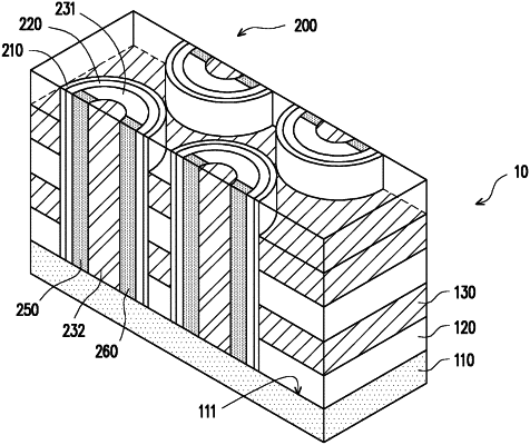
1. A memory device, comprising:
a plurality of transistor structures; and
memory arc wall structures respectively embedded in the transistor structures,
wherein each of the transistor structures comprises:
a dielectric column;
a source electrode and a drain electrode located on opposite sides of the dielectric column;
a gate electrode layer around the dielectric column, the source electrode, and the drain electrode; and
a channel wall structure extended from the source electrode to the drain electrode and surrounding the dielectric column, wherein the channel wall structure is disposed between the gate electrode layer and the source electrode, between the gate electrode layer and the drain electrode, and between the gate electrode layer and the dielectric column,
wherein each of the memory arc wall structures is extended on and throughout the channel wall structure and sandwiched between the gate electrode layer and the channel wall structure,
wherein lateral surfaces of the dielectric column, the source electrode, and the drain electrode are respectively exposed from lateral edges of the gate electrode layer.
|