| CPC H10B 43/40 (2023.02) [H01L 21/76805 (2013.01); H01L 21/76816 (2013.01); H01L 21/76826 (2013.01); H01L 21/76877 (2013.01); H01L 21/76895 (2013.01); H01L 23/5226 (2013.01); H01L 23/5283 (2013.01); H01L 23/535 (2013.01); H10B 41/41 (2023.02)] | 12 Claims |
|
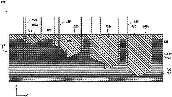
1. A method of forming a microelectronic device, the method comprising:
forming isolated nitride structures on steps of stair step structures formed in a stack structure comprising a vertically alternating arrangement of first insulative materials and second insulative materials arranged in tiers;
forming a photoresist material over a lowermost stair step structure of the stair step structures prior to forming the isolated nitride structures on the steps of the stair step structures; and
replacing the isolated nitride structures and the second insulative materials with an electrically conductive material to respectively form conductive pad structures and electrically conductive structures.
|