| CPC H10B 43/27 (2023.02) [H01L 29/40117 (2019.08); H01L 29/4234 (2013.01); H10B 43/10 (2023.02); H10B 43/35 (2023.02); H10B 43/40 (2023.02)] | 20 Claims |
|
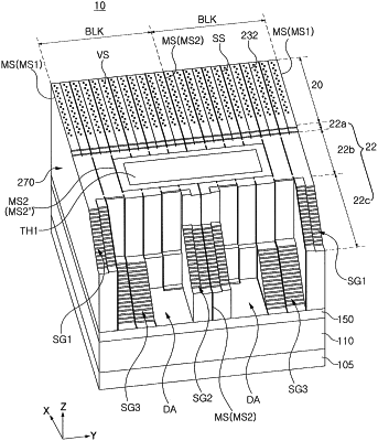
1. A three-dimensional semiconductor device, comprising:
a lower substrate;
a lower structure on the lower substrate, the lower structure including a peripheral circuit;
an upper substrate on the lower structure;
a gap-fill layer penetrating through the upper substrate;
a stack structure on the upper substrate, the stack structure including interlayer insulating layers and gate layers alternately stacked in a vertical direction, the vertical direction being perpendicular to an upper surface of the upper substrate;
a through region passing through the stack structure, at least a portion of the through region vertically overlapping the gap-fill layer;
a vertical channel structure penetrating through the stack structure;
a peripheral contact plug penetrating through the through region; and
a separation structure penetrating through the stack structure,
wherein, in a plan view, the stack structure surrounds an entire side surface of the through region,
wherein the separation structure includes a first line portion and a second line portion,
wherein the separation structure further includes a third line portion and a fourth line portion between the first line portion and the second line portion, and
wherein the fourth line portion is between the through region and the third line portion, the fourth line portion being spaced apart from the third line portion.
|