US 11,903,205 B2
Method for reading data of a first memory cell transistor of a nonvolatile semiconductor memory device
Masaru Kito, Yokohama (JP); Hideaki Aochi, Kawasaki (JP); Ryota Katsumata, Yokohama (JP); Akihiro Nitayama, Yokohama (JP); Masaru Kidoh, Kawasaki (JP); Hiroyasu Tanaka, Tokyo (JP); Yoshiaki Fukuzumi, Yokohama (JP); Yasuyuki Matsuoka, Yokohama (JP); and Mitsuru Sato, Yokohama (JP)
Assigned to Kioxia Corporation, Tokyo (JP)
Filed by Kioxia Corporation, Tokyo (JP)
Filed on May 13, 2022, as Appl. No. 17/744,571.
Application 13/064,559 is a division of application No. 11/654,551, filed on Jan. 18, 2007, granted, now 7,936,004, issued on May 3, 2011.
Application 17/744,571 is a continuation of application No. 17/141,504, filed on Jan. 5, 2021, granted, now 11,362,106.
Application 17/141,504 is a continuation of application No. 16/245,271, filed on Jan. 11, 2019, granted, now 10,916,559, issued on Feb. 9, 2021.
Application 16/245,271 is a continuation of application No. 15/666,653, filed on Aug. 2, 2017, granted, now 10,211,219, issued on Feb. 19, 2019.
Application 15/666,653 is a continuation of application No. 14/724,853, filed on May 29, 2015, granted, now 9,748,260, issued on Aug. 29, 2017.
Application 14/724,853 is a continuation of application No. 13/198,359, filed on Aug. 4, 2011, granted, now 9,064,735, issued on Jun. 23, 2015.
Application 13/198,359 is a continuation of application No. 13/064,559, filed on Mar. 31, 2011, granted, now 8,551,838, issued on Oct. 8, 2013.
Claims priority of application No. 2006-086674 (JP), filed on Mar. 27, 2006.
Prior Publication US 2022/0302166 A1, Sep. 22, 2022
This patent is subject to a terminal disclaimer.
Int. Cl. H10B 43/27 (2023.01); H01L 21/822 (2006.01); H01L 27/06 (2006.01); H01L 27/105 (2023.01); H10B 41/27 (2023.01); H10B 43/20 (2023.01); H10B 43/40 (2023.01); H10B 69/00 (2023.01); G11C 16/04 (2006.01)
CPC H10B 43/27 (2023.02) [H01L 21/8221 (2013.01); H01L 27/0688 (2013.01); H01L 27/105 (2013.01); H10B 41/27 (2023.02); H10B 43/20 (2023.02); H10B 43/40 (2023.02); H10B 69/00 (2023.02); G11C 16/0483 (2013.01)] 20 Claims
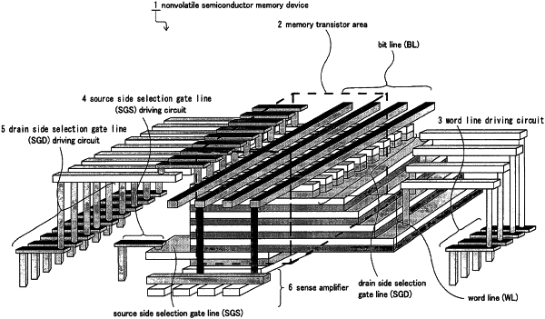
OG exemplary drawing
 
1. A method for reading data of a first memory cell transistor of a nonvolatile semiconductor memory device comprising:
applying a first voltage to a gate of a first select transistor, the first select transistor being coupled between a first bit line and a first memory unit having the first memory cell transistor and a second memory cell transistor coupled in series, the first memory cell transistor and the second memory cell transistor being arranged in a first direction crossing a surface of a substrate;
applying a second voltage lower than the first voltage to a gate of a second select transistor, the second select transistor being coupled between the first bit line and a second memory unit having a third memory cell transistor and a fourth memory cell transistor coupled in series, the third memory cell transistor and the fourth memory cell transistor being arranged in the first direction, a gate of the first memory cell transistor being coupled with a gate of the third memory cell transistor, a gate of the second memory cell transistor being coupled with a gate of the fourth memory cell transistor, the gate of the first select transistor not being coupled with the gate of the second select transistor; and
applying a read voltage to the gate of the first memory cell transistor for reading data of the first memory cell transistor and applying a pass voltage to the gate of the second memory cell transistor, the pass voltage being higher than the read voltage.