| CPC H10B 43/27 (2023.02) [H10B 43/10 (2023.02); G11C 16/0466 (2013.01)] | 19 Claims |
|
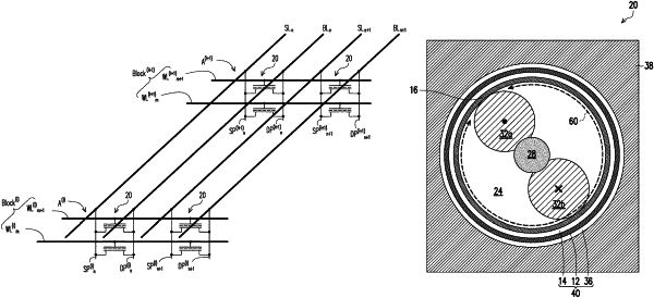
1. A 3D AND flash memory device comprising:
a gate stack structure disposed on a dielectric substrate and comprising a plurality of gate layers and a plurality of insulating layers alternately stacked with each other;
a channel pillar disposed on the dielectric substrate and penetrating through the gate stack structure;
a first conductive pillar and a second conductive pillar disposed in the channel pillar and penetrating through the gate stack structure, wherein the first conductive pillar and the second conductive pillar are separated from each other and are each connected to the channel pillar;
a charge storage structure disposed between the gate layers and a sidewall of the channel pillar; and
a protective cap covering at least a top surface of the channel pillar, isolating the first conductive pillar from a top gate layer of the plurality of gate layers, and isolating the second conductive pillar from the top gate layer of the plurality of gate layers.
|