| CPC H10B 43/27 (2023.02) [H01L 21/02164 (2013.01); H01L 21/02238 (2013.01); H01L 21/02532 (2013.01); H01L 21/02592 (2013.01); H01L 21/02667 (2013.01); H01L 23/3171 (2013.01); H01L 29/04 (2013.01); H01L 29/16 (2013.01)] | 17 Claims |
|
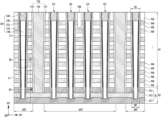
1. A semiconductor memory device comprising:
a core pillar extended in a vertical direction;
a channel layer having a first region covering a portion of a side surface of the core pillar and a second region covering an other portion of the side surface of the core pillar and a bottom surface of the core pillar, the second region positioned under the first region; and
a channel passivation layer formed in the first region of the channel layer and abutting the core pillar,
wherein the channel layer of the first region has a smaller thickness than the channel layer of the second region, and
wherein an upper surface of the channel layer of the second region is contacted with bottom surfaces of the channel layer of the first region and the channel passivation layer.
|