| CPC H10B 43/27 (2023.02) [H01L 23/5226 (2013.01); H10B 41/10 (2023.02); H10B 41/27 (2023.02); H10B 41/35 (2023.02); H10B 43/10 (2023.02); H10B 43/35 (2023.02)] | 19 Claims |
|
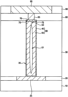
1. A through via structure comprising:
a through via including
a metal pattern, the metal pattern extending in a vertical direction and fully enclosing a gap in the metal pattern, wherein the metal pattern includes a seam extending vertically from the gap in the metal pattern, and wherein an etching gas used to form the metal pattern remains in the gap in the metal pattern,
and
a barrier pattern on a sidewall and a lower surface of the metal pattern; and
a capping pattern contacting an upper surface of the through via, the capping pattern including a lowermost edge portion, and the lowermost edge portion of the capping pattern is not higher than a lowermost central portion of the capping pattern.
|