| CPC H10B 43/27 (2023.02) [H10B 41/10 (2023.02); H10B 41/27 (2023.02); H10B 41/40 (2023.02); H10B 43/10 (2023.02); H10B 43/40 (2023.02)] | 20 Claims |
|
1. A semiconductor device comprising:
gate electrodes spaced apart from each other on a substrate and stacked in a direction perpendicular to an upper surface of the substrate;
insulating layers alternately stacked with the gate electrodes; and
channel structures that extend through the gate electrodes and the insulating layers,
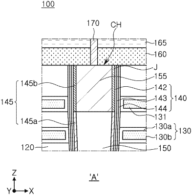
wherein ones of the channel structures comprise a channel insulating layer, a pad layer on the channel insulating layer, and a channel layer on a side surface of the channel insulating layer and on at least a portion of a side surface of the pad layer,
wherein the channel layer comprises a first channel region and a second channel region,
wherein a length of the second channel region in the direction perpendicular to the upper surface of the substrate is shorter than a length of the first channel region in the direction perpendicular to the upper surface of the substrate,
wherein the second channel region is adjacent to the pad layer and is adjacent to a first erase gate electrode that is a farthest one of the gate electrodes from the substrate,
wherein the second channel region comprises a semiconductor material doped with a first conductivity type impurity, the first channel region comprises a semiconductor material having an impurity concentration lower than an impurity concentration in the second channel region, and the pad layer comprises a semiconductor material doped with a second conductivity type impurity that is different from the first conductivity type impurity,
wherein the second channel region and the pad layer are configured to form a P-N junction therebetween, and
wherein a height level of a lower surface of the second channel region is lower than a height level of a lower surface of the first erase gate electrode.
|