| CPC H10B 43/20 (2023.02) [H01L 29/40117 (2019.08); H01L 29/66833 (2013.01); H01L 29/792 (2013.01); H10B 43/27 (2023.02); H10B 43/35 (2023.02)] | 19 Claims |
|
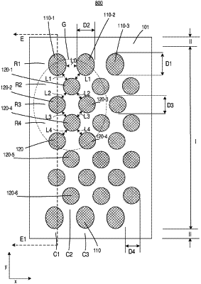
1. A semiconductor structure, comprising:
a stack structure comprising a plurality of conductor layers and a plurality of insulating layers stacking alternately along a direction perpendicular to a top surface of the stack structure; and
an array of semiconductor channels within a first region of the stack structure, wherein each semiconductor channel of the array of semiconductor channels penetrates through the stack structure, and wherein:
the array of semiconductor channels comprises:
semiconductor channels in a first row and adjacent to a second region of the stack structure, wherein the second region is adjacent to the first region; and
semiconductor channels in a second row farther away from the second region than the semiconductor channels in the first row;
a first length of a top surface of each of the semiconductor channels in the first row is greater than a second length of a top surface of each of the semiconductor channels in the second row, wherein the first length and the second length are along a first direction parallel to the top surface of the stack structure and pointing from the second region to the first region;
the first length of the top surface of each of the semiconductor channels in the first row is greater than a first width of the top surface of each of the semiconductor channels in the first row, wherein the first width is along a second direction parallel to the top surface of the stack structure and perpendicular to the first direction; and
the second length of the top surface of each of the semiconductor channels in the second row is substantially the same as a second width of the top surface of each of the semiconductor channels in the second row, wherein the second width is along the second direction.
|