| CPC H10B 41/46 (2023.02) [H01L 29/40114 (2019.08); H01L 29/42336 (2013.01); H10B 41/30 (2023.02); H01L 29/513 (2013.01)] | 20 Claims |

|
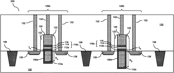
1. A method of making a MOSFET device, the method comprising:
etching a first floating gate trench in a substrate;
forming a first tunnel dielectric layer on sidewalls of the first floating gate trench;
forming a first floating gate layer in the first floating gate trench on the first tunnel dielectric layer;
planarizing the first floating gate layer, wherein a remaining portion of the first floating gate layer comprises a first floating gate electrode;
forming a first control gate dielectric layer and a first control gate electrode over the first floating gate electrode;
forming a first sidewall spacer on the first control gate dielectric layer and the first control gate electrode; and
forming a source region and a drain region each in the substrate using the first sidewall spacer as a mask, wherein a channel region continuously extends between the source region and the drain region underneath the first floating gate trench, a first p-n junction between the channel region and the source region has a first top edge that is aligned to, and adjoined to, a bottom edge a first outer sidewall of the first sidewall spacer, and a second p-n junction between the channel region and the drain region has a second top edge that is aligned to, and adjoined to, a bottom edge a second outer sidewall of the first sidewall spacer.
|