US 11,903,188 B2
Memory devices, semiconductor devices, and methods of operating a memory device
Perng-Fei Yuh, Walnut Creek, CA (US); Yih Wang, Hsinchu (TW); Meng-Sheng Chang, Hsinchu County (TW); Jui-Che Tsai, Tainan (TW); Ku-Feng Lin, New Taipei (TW); Yu-Wei Lin, Taichung (TW); Keh-Jeng Chang, Hsinchu (TW); Chansyun David Yang, Hsinchu (TW); Shao-Ting Wu, Hsinchu (TW); Shao-Yu Chou, Hsinchu County (TW); Philex Ming-Yan Fan, Tainan (TW); Yoshitaka Yamauchi, Hsinchu (TW); and Tzu-Hsien Yang, Hsinchu (TW)
Assigned to TAIWAN SEMICONDUCTOR MANUFACTURING COMPANY LTD., Hsinchu (TW)
Filed by TAIWAN SEMICONDUCTOR MANUFACTURING COMPANY LTD., Hsinchu (TW)
Filed on Feb. 16, 2022, as Appl. No. 17/673,126.
Prior Publication US 2023/0262969 A1, Aug. 17, 2023
Int. Cl. G11C 17/16 (2006.01); H10B 20/20 (2023.01); G11C 17/18 (2006.01)
CPC H10B 20/20 (2023.02) [G11C 17/16 (2013.01); G11C 17/18 (2013.01)] 20 Claims
OG exemplary drawing
 
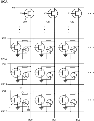
1. A memory device, comprising:
a memory cell;
a bit line connected to the memory cell;
a word line connected to the memory cell;
a select transistor in the memory cell, a gate of the select transistor connected to the word line;
a fuse element in the memory cell, the fuse element connected the select transistor; and
a heater configured to heat the fuse element, wherein the heater includes a heating transistor, and a ratio of the size of the select transistor to the size of the heating transistor is between a range from 5 to 10.