| CPC H10B 12/485 (2023.02) [H10B 12/033 (2023.02); H10B 12/053 (2023.02); H10B 12/315 (2023.02); H10B 12/34 (2023.02); H10B 12/482 (2023.02)] | 20 Claims |
|
1. A method of manufacturing a semiconductor device, comprising:
providing a substrate comprising a plurality of active areas separated from each other;
forming first mask structures on the substrate;
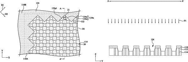
forming a first protective layer covering the first mask structures and the substrate, wherein the first protective layer defines an area exposing a portion of the first mask structures and the substrate, and the area defined by the first protective layer has a zigzag edge in a top view; and
performing a first etching process to form trenches defined by the substrate.
|