| CPC H10B 12/373 (2023.02) [H10B 12/0383 (2023.02); H10B 12/09 (2023.02); H10B 12/50 (2023.02)] | 11 Claims |

|
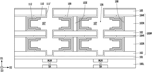
1. A method for fabricating a memory device, comprising:
forming a bit line extending vertically from a peripheral circuit portion;
forming a capacitor surrounding the bit line;
forming a transistor including a vertical active layer extending vertically from a first side of the capacitor and a word line surrounding the vertical active layer; and
forming a plate line coupled to a second side of the capacitor, and extending vertically from the peripheral circuit portion,
wherein the forming of the transistor comprises:
forming a first source/drain layer coupled to the first side of the capacitor;
forming a vertical channel layer epitaxial-grown vertically from the first source/drain layer; and
forming a second source/drain layer epitaxial-grown horizontally from the vertical channel layer, and coupled to the bit line.
|