| CPC H10B 12/34 (2023.02) [G11C 11/4023 (2013.01); H01L 29/24 (2013.01)] | 20 Claims |
|
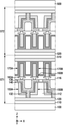
1. A semiconductor memory device comprising:
a conductive line extending in a first direction on a substrate;
an interlayer insulation film that includes a cell trench extending in a second direction intersecting the first direction, on the substrate;
a first gate electrode and a second gate electrode that are spaced apart from each other in the first direction and each extend in the second direction, inside the cell trench;
a channel layer that is inside the cell trench and is electrically connected to the conductive line, on the first gate electrode and the second gate electrode; and
a gate insulation layer interposed between the first gate electrode and the channel layer, and between the second gate electrode and the channel layer.
|