| CPC H10B 12/30 (2023.02) [G11C 5/025 (2013.01); G11C 5/10 (2013.01); H01L 27/0688 (2013.01); H10B 12/02 (2023.02)] | 22 Claims |
|
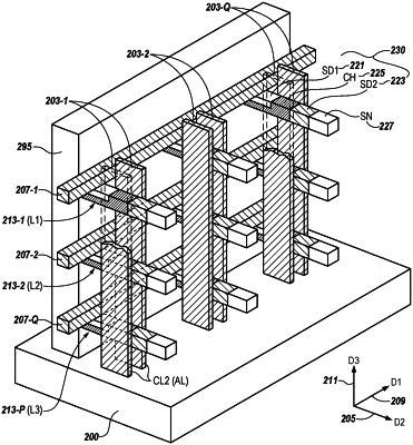
1. A memory device having arrays of vertically stacked memory cells, having multiple multi-direction conductive lines, comprising:
a vertical stack of layers formed from repeating iterations of a group of layers,
the group of layers comprising: a first dielectric material layer, a semiconductor material layer, and a second dielectric material layer, the second dielectric material layer having a conductive line formed in a horizontal plane therein; and
the vertical stack of layers having multiple multi-direction conductive lines in an interconnection region with a first portion of the interconnection region formed in an array region and a second portion formed in a conductive line contact region that is spaced from the array region.
|