| CPC H10B 12/30 (2023.02) [H01G 4/228 (2013.01); H01G 4/30 (2013.01); H01G 13/00 (2013.01); H01L 28/60 (2013.01)] | 19 Claims |
|
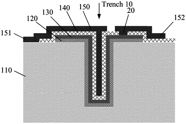
1. A capacitor, wherein the capacitor comprises:
a semiconductor substrate;
at least one trench provided in the semiconductor substrate and formed downward from an upper surface of the semiconductor substrate;
a first conductive layer provided above the semiconductor substrate and in the trench;
a first insulating layer provided between the semiconductor substrate and the first conductive layer to isolate the first conductive layer from the semiconductor substrate;
a second conductive layer provided above the semiconductor substrate and in the trench, the second conductive layer comprising a first conductive region and a second conductive region that are independent from each other, the first conductive region being electrically connected to the semiconductor substrate, and the second conductive region being electrically connected to the first conductive layer; and
a second insulating layer provided between the first conductive layer and the second conductive layer to isolate the first conductive region from the first conductive layer and isolate the second conductive region from the semiconductor substrate;
at least one conductive layer provided above the semiconductor substrate and in the trench, and located between the first conductive layer and the second conductive layer; and
at least one insulating layer provided between different conductive layers of the at least one conductive layer to isolate the at least one conductive layer respectively, and provided between the second conductive layer and the at least one conductive layer to isolate the second conductive region from the at least one conductive layer and isolate the second conductive region from the semiconductor substrate.
|