| CPC H10B 12/09 (2023.02) [H10B 12/0335 (2023.02); H10B 12/315 (2023.02); H10B 12/34 (2023.02)] | 14 Claims |
|
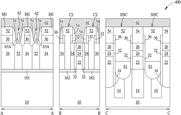
1. A semiconductor structure, comprising:
a substrate comprising a peripheral region and a memory region defined thereon;
a first dielectric layer disposed on the substrate;
a second dielectric layer disposed on the first dielectric layer;
an opening on the peripheral region of the substrate and having a lower portion through the first dielectric layer and an upper portion through the second dielectric layer;
a conductive layer disposed on the second dielectric layer at two sides of the opening;
a contact structure disposed in the lower portion of the opening;
a passivation layer covering a top surface of the contact structure, a sidewall of the second dielectric layer, and a sidewall of the conductive layer;
a plurality of bit lines disposed on the memory region of the substrate; and
a plurality of storage node contacts disposed on the substrate and between the bit lines, wherein a top surface of the conductive layer is flush with top surfaces of the storage node contacts.
|