| CPC H05K 3/363 (2013.01) [H05K 1/0277 (2013.01); H05K 1/111 (2013.01); H05K 1/115 (2013.01); H05K 1/144 (2013.01); H05K 2201/09609 (2013.01); H05K 2203/043 (2013.01)] | 12 Claims |

|
1. An electronic device comprising:
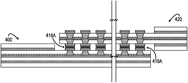
a first flexible printed circuit comprising a two-dimensional pattern of contacts on a first surface, wherein the two-dimensional pattern of contacts comprises a contact density between 0.5 contacts/mm2 and 4.0 contacts/mm2;
a second flexible printed circuit comprising a corresponding two-dimensional pattern of vias; and
a plurality of solder joints, each solder joint formed between a contact of the two-dimensional pattern of contacts and a corresponding via of the corresponding two-dimensional pattern of vias.
|