| CPC H05K 3/321 (2013.01) [G02B 7/02 (2013.01); G03B 17/12 (2013.01); H04N 23/54 (2023.01); H04N 23/60 (2023.01); H05K 1/11 (2013.01)] | 20 Claims |

|
1. A camera device comprising:
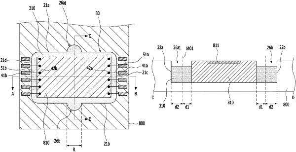
a circuit board having therein a seating recess;
an image sensor disposed in the seating recess in the circuit board; and
first epoxy disposed in the seating recess,
wherein the seating recess has first and second lateral surfaces that face each other and third and fourth lateral surfaces that face each other,
wherein the circuit board comprises a plurality of terminals disposed in an area thereof that abuts on the third and fourth lateral surfaces of the seating recess and electrically connected to the image sensor,
at least one application groove formed in at least one of the first and second lateral surfaces of the seating recess,
wherein the at least one application groove has an opening, which is formed in an upper surface of the circuit board, and
wherein at least a portion of the first epoxy is disposed in the at least one application groove.
|