US 11,903,138 B2
Fine feature formation techniques for printed circuit boards
Eric Li, Chandler, AZ (US); Kemal Aygun, Tempe, AZ (US); Kai Xiao, Portland, OR (US); Gong Ouyang, Olympia, WA (US); and Zhichao Zhang, Chandler, AZ (US)
Assigned to Intel Corporation, Santa Clara, CA (US)
Filed by INTEL CORPORATION, Santa Clara, CA (US)
Filed on Jul. 22, 2021, as Appl. No. 17/383,084.
Application 17/383,084 is a continuation of application No. 16/081,487, granted, now 11,089,689, previously published as PCT/US2016/025772, filed on Apr. 2, 2016.
Prior Publication US 2021/0352807 A1, Nov. 11, 2021
Int. Cl. H05K 1/02 (2006.01); H05K 1/16 (2006.01); H05K 3/00 (2006.01); H05K 3/02 (2006.01); H05K 3/46 (2006.01)
CPC H05K 3/0026 (2013.01) [H05K 1/0228 (2013.01); H05K 3/027 (2013.01); H05K 3/4694 (2013.01); H05K 2201/09227 (2013.01); H05K 2201/09727 (2013.01); H05K 2203/107 (2013.01); H05K 2203/1476 (2013.01)] 24 Claims
OG exemplary drawing
 
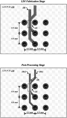
1. An apparatus, comprising:
a low density interconnect (LDI) printed circuit board (PCB); and
one or more fine conductive features disposed on the LDI PCB formed from a conductive feature, wherein the conductive feature comprising a fine gap region devoid of conductive material.