| CPC H05K 1/181 (2013.01) [H01F 10/265 (2013.01); H01F 17/0033 (2013.01); H01F 27/24 (2013.01); H01F 27/2804 (2013.01); H01F 41/02 (2013.01); H01F 41/041 (2013.01); H01F 41/046 (2013.01); H01F 41/32 (2013.01); H01L 28/10 (2013.01); H05K 1/0298 (2013.01); H05K 1/115 (2013.01); H05K 1/165 (2013.01); H01F 2017/0066 (2013.01); H05K 1/0233 (2013.01); H05K 1/0306 (2013.01); H05K 2201/086 (2013.01); H05K 2201/0929 (2013.01); H05K 2201/1003 (2013.01); Y02P 70/50 (2015.11); Y10T 29/4913 (2015.01)] | 16 Claims |
|
1. A method of manufacturing comprising:
depositing a magnetic material over a semiconductor substrate to form a magnetic layer, wherein at least a portion of a multilevel wiring network is formed on the semiconductor substrate;
in a physical vapor deposition (PVD) chamber, depositing a non-magnetic layer on the magnetic layer, wherein said non-magnetic layer is formed by:
depositing an interface material to form a first interface layer on the magnetic layer;
flowing a reactive gas into the PVD chamber, while continuing to deposit the interface material, to form an insulating material on the first interface layer, the insulating layer comprising a compound of the interface material and the reactive gas; and
stopping the reactive gas flow into the PVD chamber, while continuing to deposit the interface material, to form a second interface layer on the insulating layer;
repeating in alternate fashion, up to 100 times each, (a) the depositing of the magnetic material and (b) the depositing of the non-magnetic layer to form an alternating sequence of magnetic layers and non-magnetic layers;
depositing the magnetic material on the last non-magnetic layer in the sequence to form a final magnetic layer, resulting in a magnetic member with a laminated configuration;
masking and patterning said magnetic member in such a manner that after said patterning a remaining portion of said magnetic member comprises a planar magnetic core; and
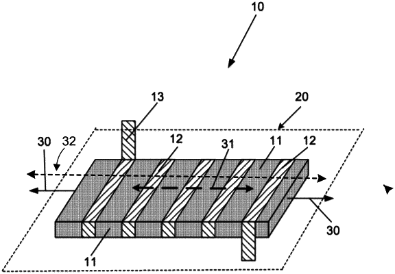
forming a conductive winding around the planar magnetic core, the conductive winding comprising wire segments and vertical interconnect accesses (VIAs), wherein said wire segments pertain to at least two wiring planes in said multilevel wiring network and said VIAs interconnect the at least two wiring planes.
|