| CPC H05K 1/119 (2013.01) [H05K 1/183 (2013.01); H05K 3/0035 (2013.01); H05K 3/0038 (2013.01); H05K 3/0044 (2013.01); H05K 2201/09827 (2013.01); H05K 2201/09854 (2013.01)] | 9 Claims |
|
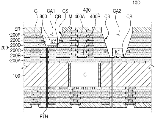
1. A printed circuit board comprising:
a first insulating material; and
a second insulating material disposed on one surface of the first insulating material in a stacking direction, and including first and second cavities having depths different from each other,
wherein at least one groove portion is disposed in a side surface, and spaced apart in the stacking direction from a bottom surface, of each of the first and second cavities, and
wherein the at least one groove portion includes an end portion covered by the second insulating material in a direction perpendicular to the stacking direction.
|