| CPC H05K 1/0219 (2013.01) [H01P 3/08 (2013.01); H05K 1/0224 (2013.01); H05K 1/0227 (2013.01); H05K 1/05 (2013.01); H05K 1/0218 (2013.01); H05K 1/0298 (2013.01); H05K 1/11 (2013.01); H05K 1/18 (2013.01)] | 13 Claims |

|
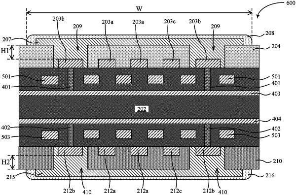
1. A printed circuit board, comprising:
a substrate having a top surface and a bottom surface;
a reference plane embedded in the substrate and adjacent to the top surface;
a first signal net disposed within a specific region on the top surface of the substrate;
a second signal net in close proximity to the first signal net and disposed within the specific region on the top surface of the substrate;
an outermost insulating layer disposed on the top surface of the substrate to cover the substrate, the first signal net and the second signal net, wherein the outmost insulating layer comprises an opening to expose a portion of the second signal net;
a conductive layer disposed in the opening and on the outermost insulating layer corresponding to the specific region in which the first signal net and the second signal net are arranged, such that the conductive layer overlaps with the first signal net; and
a fifth signal net embedded in the substrate and between the reference plane and the outermost insulating layer, wherein a top side and a bottom side of the fifth signal net are covered by the substrate,
a second reference plane embedded in the substrate and adjacent to the bottom surface;
a third signal net and a fourth signal net being in close proximity to each other and disposed within a second specific region on the bottom surface of the substrate;
a bottom outermost insulating layer disposed on the bottom surface of the substrate to cover the substrate, the third signal net and the fourth signal net, wherein the bottom outmost insulating layer comprises a second opening to expose a portion of the fourth signal net; and
a bottom conductive layer disposed in the second opening and on the bottom outermost insulating layer corresponding to the second specific region in which the third signal net and the fourth signal net are arranged, such that the bottom conductive layer overlaps with the third signal net.
|